
Solution for Substrate/epitaxial wafer EPD dislocation Inspection
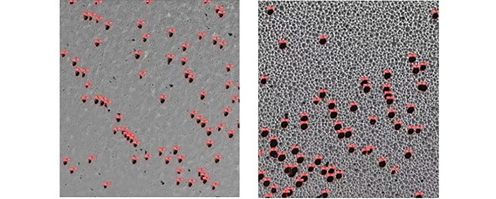
The shape and distribution of dislocation defects in the preparation of semiconductor wafers have a great impact on the performance of electronic components. Due to different doping materials and preparation processes, the dislocation distribution is also different. This solution is mainly aimed at the shape and distribution of wafer dislocations, and is committed to providing data support for wafer material research and improvement of preparation process. It is applicable to 2-inch, 3-inch, 4-inch and 6-inch GaAs substrates.

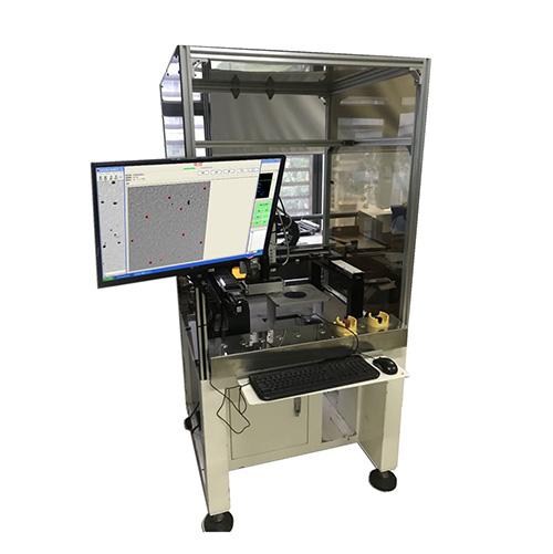
Convenient and efficient surface defect detection equipment for wafers, substrates and epitaxial wafers. Main defects: dislocations, particles, pits, scratches, stains, etc.

It replaces manual sampling inspection and greatly improves the detection efficiency and accuracy.

Check the dislocation density, morphology and distribution of the substrate and epitaxial wafer to provide data support for substrate material research, defect traceability, and improvement of preparation process;
Automatic image acquisition and artificial intelligence analysis tools.

Reliable equipment, long trouble free working time, fast response+high-quality after-sales service.

The shape and distribution of dislocation defects in semiconductor wafer preparation have a significant impact on the performance of electronic components. Due to differences in doping materials and preparation processes, the distribution of dislocations also varies. This device is used to inspect the morphology and distribution of wafer dislocations, providing data support for wafer material research and improving preparation processes. Suitable for 2-inch, 3-inch, 4-inch, and 6-inch gallium arsenide substrates.
View More Address:Unit 204, No. 30 Guanri Road, Phase II Software Park, Xiamen City
Factory Address:1st Floor,Great Wall Business Building,76-78 Huli Avenue,Xiamen City
Address:Unit 204, No. 30 Guanri Road, Phase II Software Park, Xiamen City
Factory Address:1st Floor,Great Wall Business Building,76-78 Huli Avenue,Xiamen City
 Consultation Hotline:86-0592-3799658、86-137 9991 1773(Switchboard)
 Email : AOI@otek.com.cn